The Digital Workhorse: A Deep Dive into How GPUs Actually Work
From Pixels to Parallel Powerhouse
When you marvel at the lifelike rain in a video game, instantly apply a filter to a photo, or watch a smooth 4K video, you’re witnessing the work of one of the most complex and ingenious pieces of consumer technology: the Graphics Processing Unit, or GPU. Often misunderstood as just a “video card,” a modern GPU is a specialized supercomputer designed for one core task: massive parallel processing. This article will dissect the anatomy of a GPU, moving beyond marketing specs to explain the fundamental architecture that makes real-time graphics and modern artificial intelligence possible.
The Core Philosophy: Why a GPU Isn’t Just a Faster CPU
To understand a GPU, you must first understand the problem it solves. A Central Processing Unit (CPU) is a generalist—a “commanding officer” designed for complex, sequential tasks (running your operating system, executing program logic, making decisions). It has a few, very powerful cores optimized for high single-threaded performance and rapid task switching.
A GPU is a specialist army. Its job is to perform millions of simple, repetitive mathematical calculations simultaneously. Rendering a single frame at 1080p resolution involves determining the color, lighting, and position for over 2 million pixels, and doing so 60 or 144 times per second. A CPU would choke on this; a GPU thrives on it.
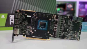
The Physical Anatomy: A Tour of the Graphics Card
A consumer graphics “card” is the entire package you plug into your PC. The GPU is the specific silicon chip at its heart.
1. The GPU Silicon Die:
This is the processor itself, manufactured by TSMC or Samsung on cutting-edge processes (e.g., 5nm, 4nm). It’s a vast expanse of transistors partitioned into key areas.
2. Streaming Multiprocessors (SMs) / Compute Units (CUs):
These are the fundamental building blocks. An NVIDIA “Ada Lovelace” GPU might have 128 SMs, while an AMD “RDNA 3” GPU has 96 Compute Units. Each SM/CU contains:
Cores (CUDA Cores / Stream Processors): The basic arithmetic logic units (ALUs) that perform the floating-point and integer math. They are simpler than CPU cores but exist in overwhelming numbers.
Schedulers/Warps: Manage the thousands of parallel threads, feeding data to the cores with incredible efficiency to keep them saturated with work.
Registers & Local Cache: Extremely fast memory directly on the SM for holding the data currently being processed.
3. The Memory Subsystem: VRAM & Bus
VRAM (Video RAM): High-speed memory (GDDR6X, GDDR7) mounted around the GPU. It acts as the frame buffer (holding completed frames), texture memory (storing surface details), and general workspace. More VRAM allows for higher resolutions and more detailed textures.
Memory Bus & Bandwidth: The width of the highway connecting the GPU to VRAM (e.g., 256-bit, 384-bit). Combined with memory speed, this determines bandwidth (GB/s)—the critical rate at which the GPU can access this data. A bottleneck here cripples performance.
4. The Render Output Pipeline (ROPs) / Render Back-Ends:
These units handle the final steps of the graphics pipeline. They write the final pixel data to the frame buffer, perform operations like anti-aliasing (smoothing jagged edges), and handle depth (Z-culling) to avoid processing pixels hidden behind objects.
5. The Interconnect: PCIe Interface
The card connects to the motherboard via a PCI Express (PCIe) slot. While crucial for data transfer with the CPU and system RAM, modern PCIe 4.0/5.0 slots provide more than enough bandwidth for most games, making the interface less of a bottleneck than in the past.
6. Cooling Solution (Fans, Heatsink, Vapor Chamber):
A high-end GPU can consume over 400 watts of power, transforming almost all of it into heat. The massive heatsink, heat pipes, vapor chamber, and fans are essential to prevent thermal throttling and maintain performance.
7. Power Delivery (VRMs):
The Voltage Regulator Module (VRM) is a sophisticated multi-phase circuit that converts power from the PCIe slot and external PCIe power connectors (6+2 pin) into clean, stable voltages the GPU silicon requires. A robust VRM is key for overclocking and stability.
The Software Magic: The Graphics Pipeline
Hardware is useless without instructions. The GPU executes a programmed sequence known as the graphics rendering pipeline. Here’s a simplified view of its key stages:
1. Vertex Shading:
The 3D world is defined by vertices (the corners of triangles). The GPU takes these vertices and processes their positions—applying transformations for perspective, animation, and camera view. This stage answers: “Where is everything in this scene from the camera’s point of view?”
2. Rasterization & Triangle Setup:
The transformed 3D triangles are “projected” onto the 2D screen space and converted (rasterized) into fragments—candidate pixels that will be filled in. This stage answers: “Which pixels on my screen are covered by each triangle?”
3. Pixel/Fragment Shading:
This is the most computationally heavy and visually impactful stage. For each fragment, the shader program calculates its final color. This involves incredibly complex math: applying textures (surface images), simulating lighting (shadows, reflections, ambient occlusion), and calculating material properties (roughness, metallicity). Modern techniques like ray tracing add another layer here, simulating the physical path of light for hyper-realistic reflections and shadows.
4. Output Merging:
The final stage combines all the shaded fragments. The ROPs handle depth testing (discarding fragments behind others), blending (for transparency effects), and finally writing the pixel to the frame buffer. The completed frame is then sent to your display.
Beyond Polygons: The General-Purpose GPU (GPGPU)
The GPU’s parallel architecture is so effective that its use has exploded beyond graphics. This is called General-Purpose computing on GPU (GPGPU), powered by platforms like NVIDIA’s CUDA and the open-standard OpenCL.
AI & Machine Learning: Training and running neural networks involves massive matrix multiplications—a perfect parallel task. Modern GPUs include specialized Tensor Cores (NVIDIA) or Matrix Cores (AMD) that accelerate this math exponentially.
Scientific Simulation & Research: Modeling weather, protein folding (see Folding@home), or financial markets.
Video Encoding/Decoding: Dedicated media engines on GPUs (NVENC, AMD VCE) use parallel processing to encode video streams for recording, streaming, or video calls with high efficiency.
Conclusion: More Than Just Frames Per Second
Understanding the GPU’s anatomy reveals why it’s a cornerstone of modern computing. It is a masterpiece of specialized engineering: a chip designed not for making decisions, but for executing a singular, parallelizable vision with brute-force efficiency. From painting the pixels in your favorite game to training the AI that might diagnose an illness, the GPU’s journey from a simple rasterizer to a general-purpose parallel powerhouse is one of the most significant evolutions in computing history. When you look at a graphics card, you’re no longer just looking at a component for gaming—you’re looking at a window into the parallelized future of computation itself.